Electronics Design
Individual Assignment:
- Utilize an Electronic Design Automation (EDA) tool to design a development board capable of interacting and communicating with an embedded microcontroller.
- Produce the designed board and conduct thorough testing.
Extra Credit Tasks:
- Explore an alternative design workflow for the development board.
- Design a case for the development board to enhance its physical protection and aesthetics.
- Simulate the operation of the development board to ensure its functionality and performance.
Group Assignment: click here
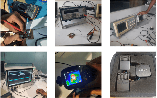
- Utilize the test equipment available in our lab to observe the operation of a microcontroller circuit board.
- Send a PCB (Printed Circuit Board) out to a board house.
This week's group assignment involved using the test equipment in our lab to observe the operation of a microcontroller circuit board.
Here are some basic electronic components commonly used in circuits:
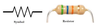
Resistor : A passive two-terminal component that restricts the flow of electric current. It is commonly used to adjust signal levels, terminate transmission lines, and divide voltages.
Capacitor : A passive two-terminal component that stores electrical energy in an electric field. It is used in various applications such as filtering, decoupling, energy storage, and timing circuits.

Inductor : A passive two-terminal component that stores energy in a magnetic field when current flows through it. It is commonly used in filtering, impedance matching, and energy storage applications.

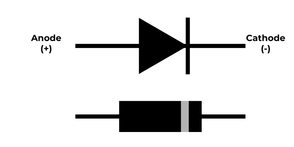
Diode : A semiconductor device that allows current to flow in one direction only. It is used in rectification, signal demodulation, voltage regulation, and switching applications.
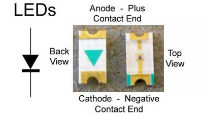
LED (Light-Emitting Diode) : A semiconductor light source that emits light when current flows through it. It is commonly used as indicators, in displays, and for lighting purposes.
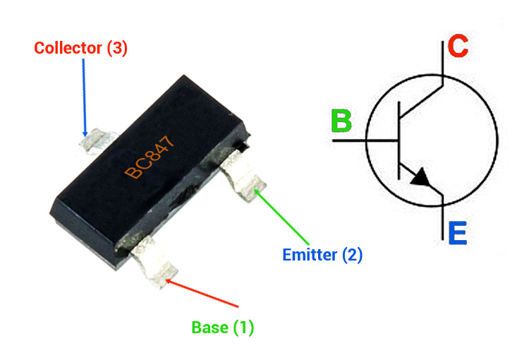
Transistor : A semiconductor device that amplifies or switches electronic signals and electrical power. There are different types of transistors including bipolar junction transistors (BJTs) and field-effect transistors (FETs).
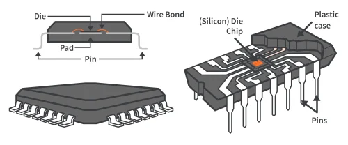
Integrated Circuit (IC) : A miniaturized electronic circuit consisting of semiconductor devices and passive components fabricated onto a small chip of semiconductor material. ICs can perform various functions such as amplification, signal processing, and digital logic operations.
Switch : A mechanical or electronic device that interrupts or redirects the flow of electrical current. Switches are used to control circuits, turning them on or off.
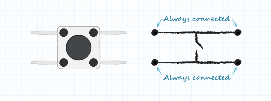
In our electronic design, we utilize simple tactile push-to-ON switches for instant inputs,
When connecting a push button to a microcontroller as an input device, we implement either a pull-up or pull-down resistor to mitigate noise at the microcontroller's input pin. Without these resistors, the input pin may experience floating behavior between ground (GND) and power (VCC), resulting in unpredictable input if the switch is not active. By incorporating pull-up or pull-down resistors, we stabilize the input signal and ensure reliable operation of the switch with the microcontroller.
PCB designing
PCB designing, also known as electronic design automation (EDA) software, is essential for creating schematic diagrams, printed circuit board (PCB) layouts, and conducting circuit simulations. Here are some popular EDA software tools:
- Fusion 360
- Eagle CAD
- KiCad
- OrCAD
- EasyEDA
- Altium Designer
Each of these tools offers unique features and capabilities, catering to various requirements and preferences of electronics designers
For this week, I've decided to use KiCad for designing my PCB.
KiCad is an open-source Electronic Design Automation (EDA) software. This tool enables users to create schematic diagrams of electronic circuits and seamlessly convert them into PCB layouts. To download KiCad, click here
The initial step is to begin with the schematic diagram of the circuit.
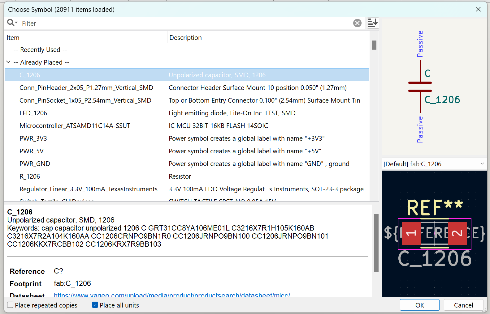
I've created a new project.To access Fab Academy's library of symbols and footprints for KiCad, I downloaded the .zip file from the provided link:
https://gitlab.fabcloud.org/pub/libraries/electronics/kicad
To insert the symbols file into KiCad, follow these steps:
- Open KiCad.
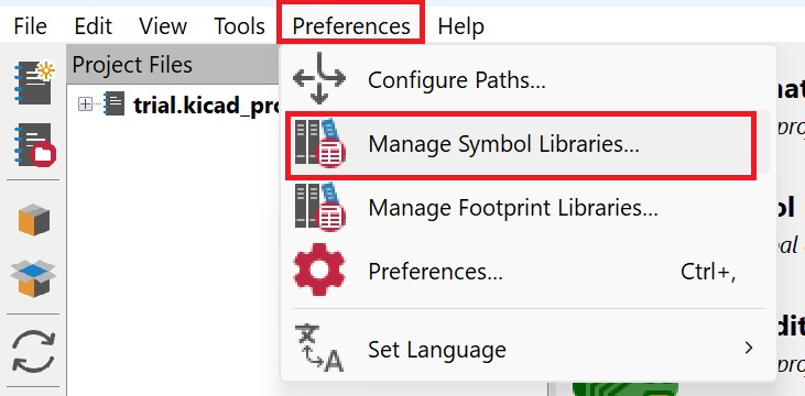
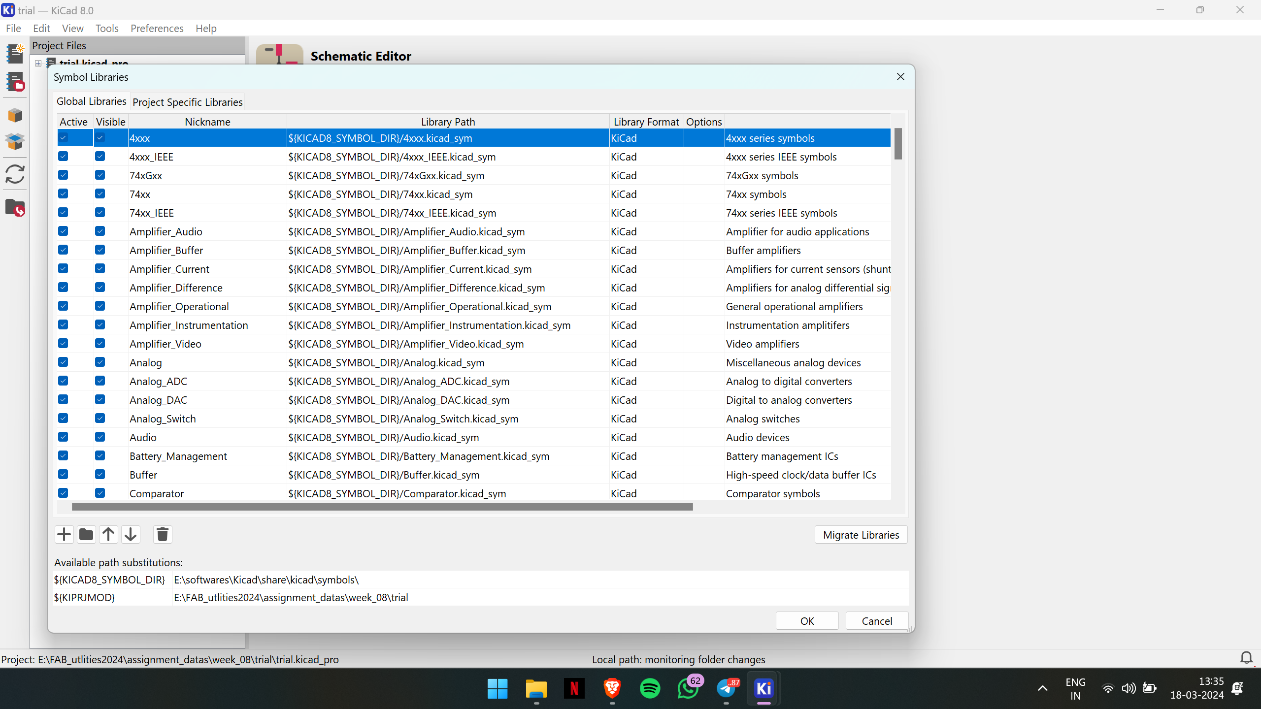
- Navigate to Preferences > Manage Symbol Libraries
- Click on "Add file" and select the downloaded symbols file from your computer.
To insert the footprints file into KiCad, follow these steps:
- Open KiCad.
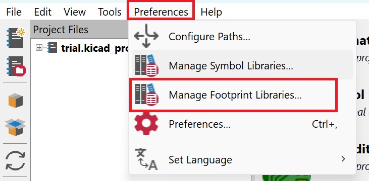
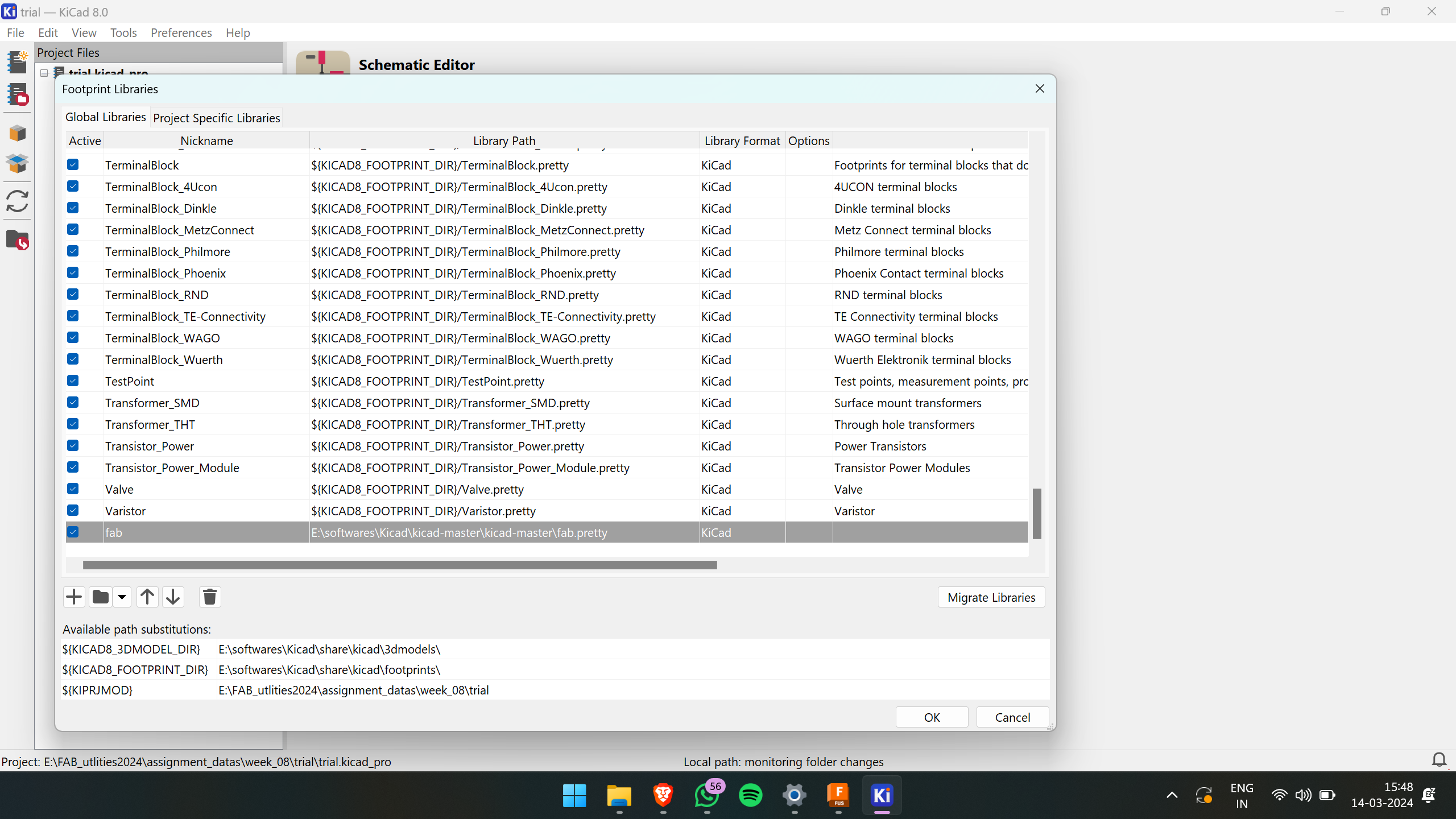
- Go to Preferences > Manage Footprints Libraries.
- Click on "Add file" and select the downloaded footprints file from your computer.
This will integrate Fab Academy's symbols and footprints library into your KiCad project, allowing you to access them for the schematic design and PCB layout.
For this week's project, I've selected the SAMD11C microcontroller for my design. The SAMD11C is part of a series of low-power microcontrollers based on the ARM architecture
Features of SAMD11C:
- Microcontroller Core : ARM Cortex-M0+ CPU running at up to 24 MHz clock frequency.
- Memory : Flash, SRAM, and EEPROM for program and data storage.
- Peripherals : USART, SPI, I2C communication interfaces, ADC, timers, analog comparators, capacitive touch sensing.
- GPIO (General Purpose Input/Output) : Configurable pins for interfacing with external devices.
- Clock Management : Integrated clock sources and PLLs for generating system clocks.
- Power Management : Multiple low-power modes to conserve energy.
- Security Features : Hardware-accelerated AES encryption for secure communication.
- Packages : Available in various package options including QFN, TQFP, and SOIC.
- Voltage Range : Typically operates from 1.8V to 3.6V.
- Temperature Range : Operating temperature range typically from -40°C to 85°C or wider depending on the variant.
- Applications : Suitable for IoT, home automation, industrial automation, and more.
After opening the schematic file, I began adding the necessary components for my design. By pressing "a," I accessed the symbols, all of which were conveniently located under the "fab" group.
Here is the S chematic diagram after adding and connecting the necessary components.
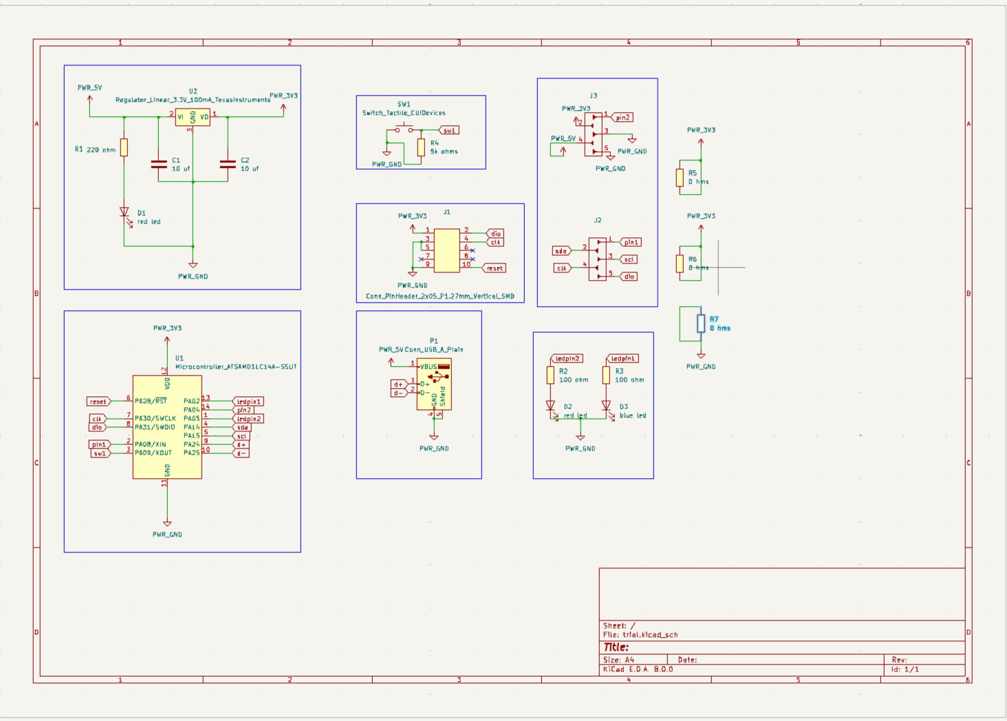
| Sl No: | Reference | Value | Qunatity |
|---|---|---|---|
| 1 | C1, C2 | 10 uf | 2 |
| 2 | R5, R6, R7 | 0 hms | 3 |
| 3 | R2, R3 | 100 ohm | 2 |
| 4 | R1 | 220 ohm | 1 |
| 5 | R4 | 5k ohms | 1 |
| 6 | D1, D2 | red led | 2 |
| 7 | D3 | blue led | 1 |
| 8 | U1 | Microcontroller_ATSAMD11C14A-SSUT | 1 |
| 9 | U2 | Regulator_Linear_3.3V_100mA_TexasInstruments | 1 |
| 10 | SW1 | Switch_Tactile_CUIDevices | 1 |
| 11 | J2, J3 | Conn_PinSocket_1x05_P2.54mm_Vertical_SMD | 2 |
| 12 | J1 | Conn_PinHeader_2x05_P1.27mm_Vertical_SMD | 1 |
| 13 | P1 | Conn_USB_A_Plain | 1 |
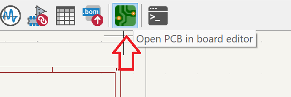
Once the schematic diagram was complete, the next step was to design the PCB and add the traces. To do this, click on the "Open PCB in board editor" icon located at the top right corner.
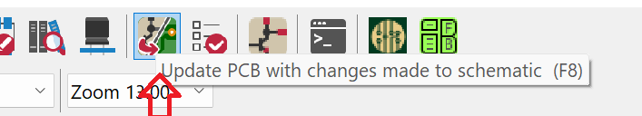
Upon opening the PCB editor, a new screen appears. To update the PCB with the changes made in the schematic, click on the "Update PCB with changes made to schematic" icon located at the top right corner. Then press "Update PCB" to synchronize the changes between the schematic and the PCB layout.
The next step involves defining the constraints and parameters for PCB design.
To add the constraints, navigate to the board setup menu and select "Constraints." This allows you to define specific design parameters

Based on the capabilities of our milling machine identified during the "Electronics Production" week, the values are as follows:
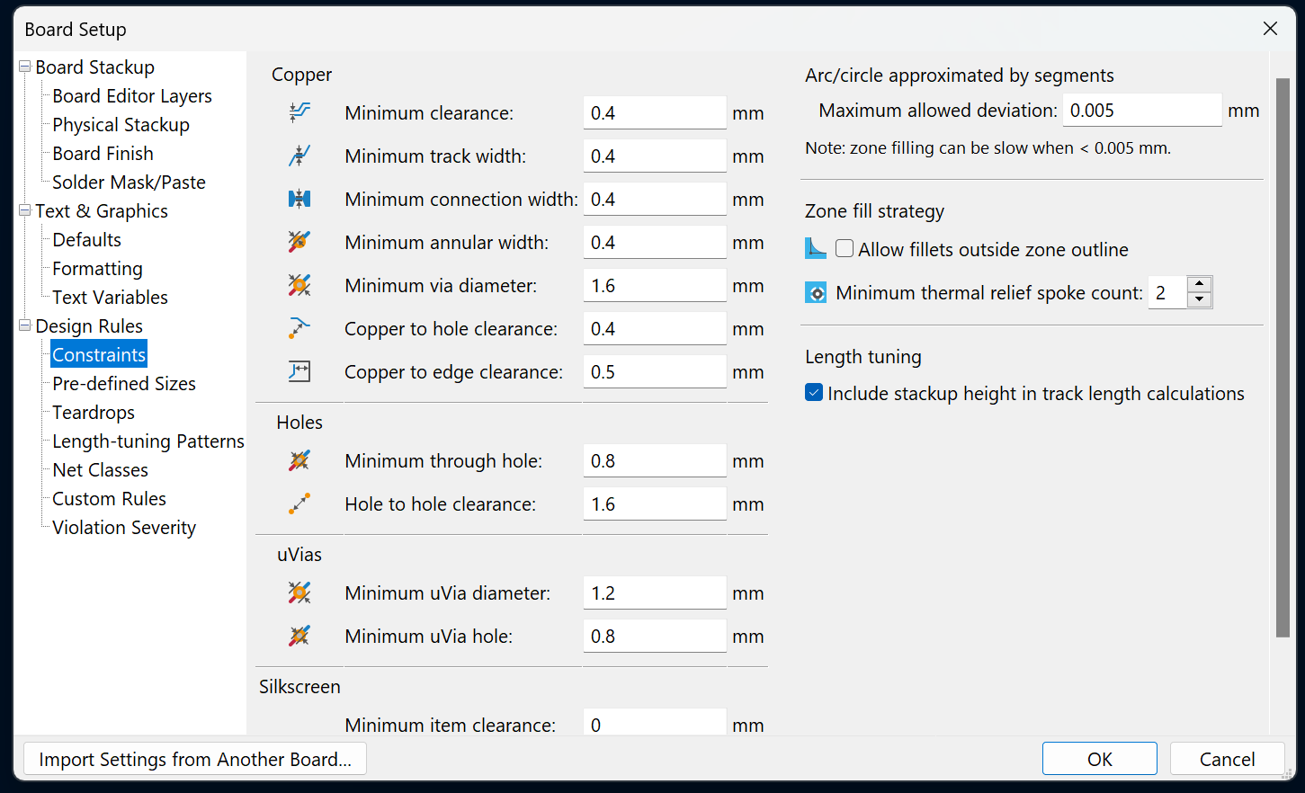
These constraints and parameters ensure compatibility with our milling machine's capabilities and allow for accurate fabrication of the PCB.
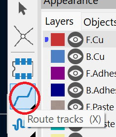
After adding the constraints, we can proceed to route the PCB. To do this, we can choose the routing tool from the sidebar, or simply click the "X" button on the keyboard. This allows us to begin the process of laying out and connecting the traces on the PCB.
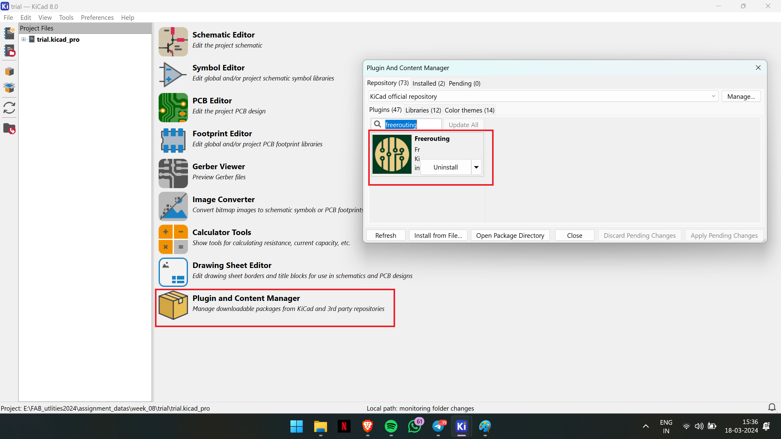
Initially, I attempted manual routing, but found it to be time-consuming. At this point, I discovered the auto-routing plugin in KiCad and decided to add it to expedite the routing process.
To add the auto-routing plugin in KiCad, follow these steps:
- Navigate to the main window of KiCad.
- Go to "Plugin" and select "Plugin and Content Manager."
- In the Plugin and Content Manager, search for "FreeRouting."
- Select the FreeRouting plugin and add it to your KiCad installation.
Once the FreeRouting plugin is installed, you can access it from the main window of KiCad to assist in the routing process.
When encountering an issue with the track width during auto-routing, such as finding it set to 0.2 while my required track width is 0.4, I researched and discovered that the default parameters for auto-routing may differ. To address this, I navigated to the board manager and adjusted the values in the net class as follows:
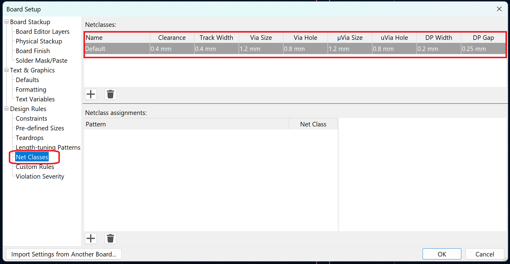
- Open the board manager.
- Navigate to the net class settings.
- Adjust the parameters
This ensures that the auto-routing adheres to the correct track width required for the design.
During the auto-routing process for my design, the auto-router initially proposed a two-layer routing solution. Determined to achieve a single-layer layout, I challenged the auto-router's decision😒 and attempted manual routing. However, after realizing the complexity of the circuit, I acknowledged the necessity of the two-layer solution.🥹
To maintain a single-layer design, I strategically added three 0-ohm resistors to facilitate track jumps across specific routes😌. This adjustment allowed me to successfully complete the routing while adhering to design constraints and ensuring the circuit's intended functionality.
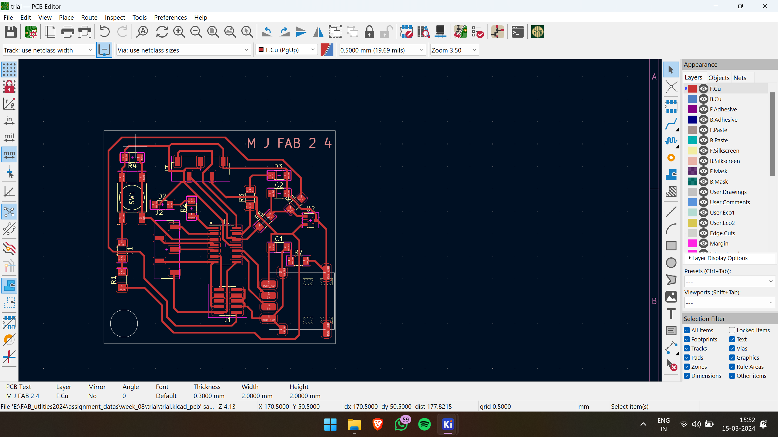
Here is the output after completing the routing procedure.
The next step is to export the PCB design in Gerber format. This format is commonly used for manufacturing printed circuit boards (PCBs).
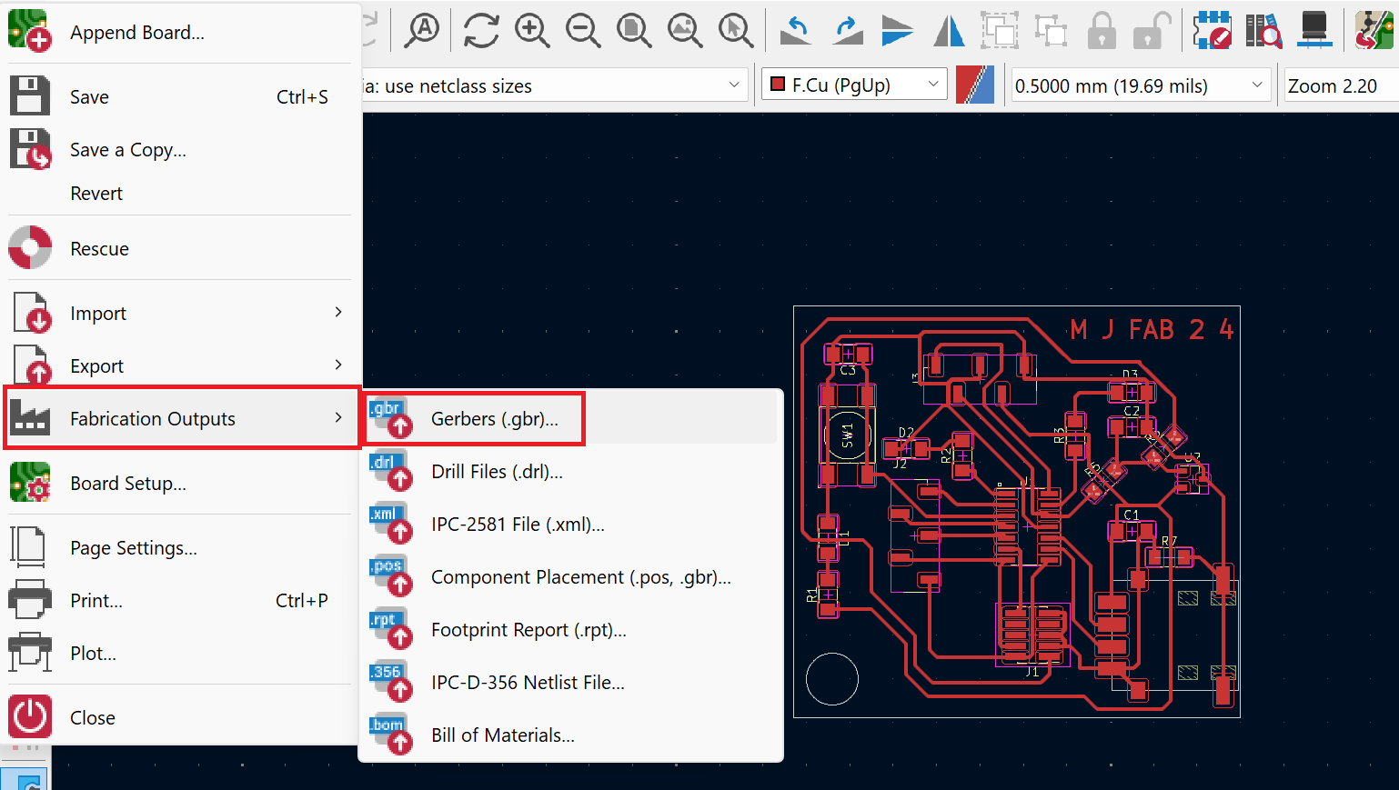
To export the PCB design in Gerber format, follow these steps:
- Go to "File" in the menu bar.
- Select "Fabrication Outputs."
- Choose "Gerbers" from the options.
This will generate the Gerber files required for PCB fabrication.
The next step involves converting the Gerber file into a PNG format suitable for the milling process.
I utilized a web application developed by our own SuperFabLab team, which simplifies the conversion of Gerber files to PNG format. This streamlined process facilitates easy conversion for the milling process.
To access the web application, please use the following link: https://gerber2png.fablabkerala.in/
This is the landing page of the web application designed by our SuperFabLab team for converting Gerber files to PNG format.
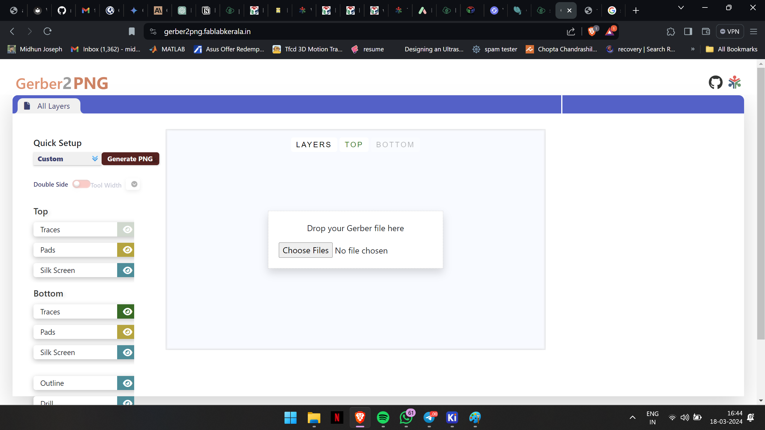
In this web application, you can upload the Gerber file. On the top left corner, there is an option for selecting the top layer for the traces
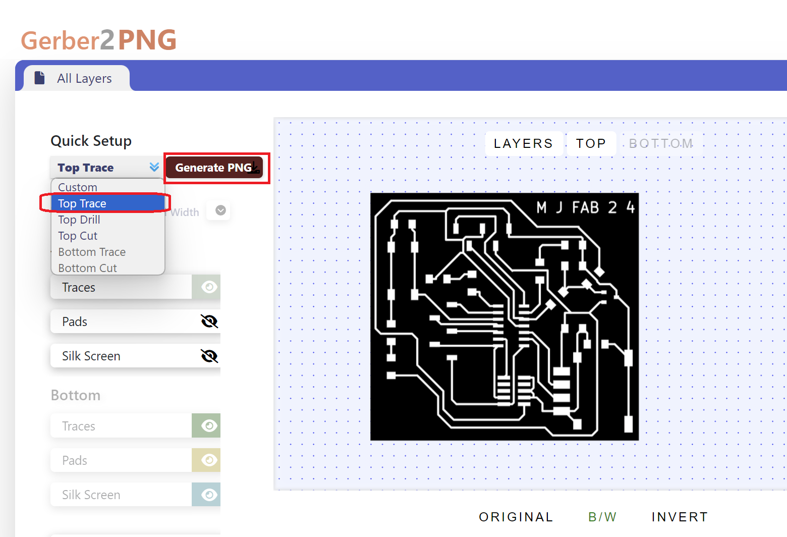
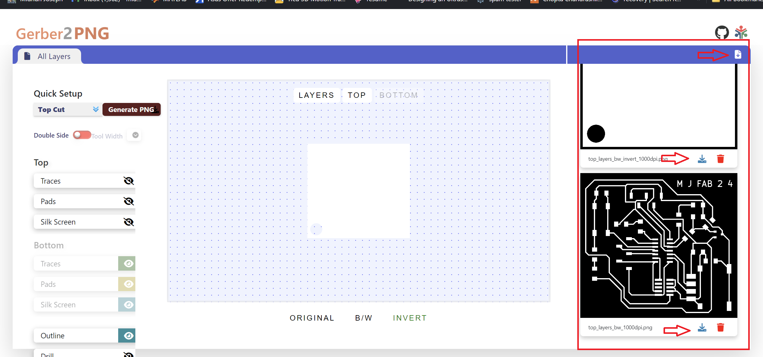
After selecting the " Generate PNG " option, the web application will generate the PNG file, which can be downloaded and utilized for milling purposes.
For the cut file, select the "Top Cut" option.
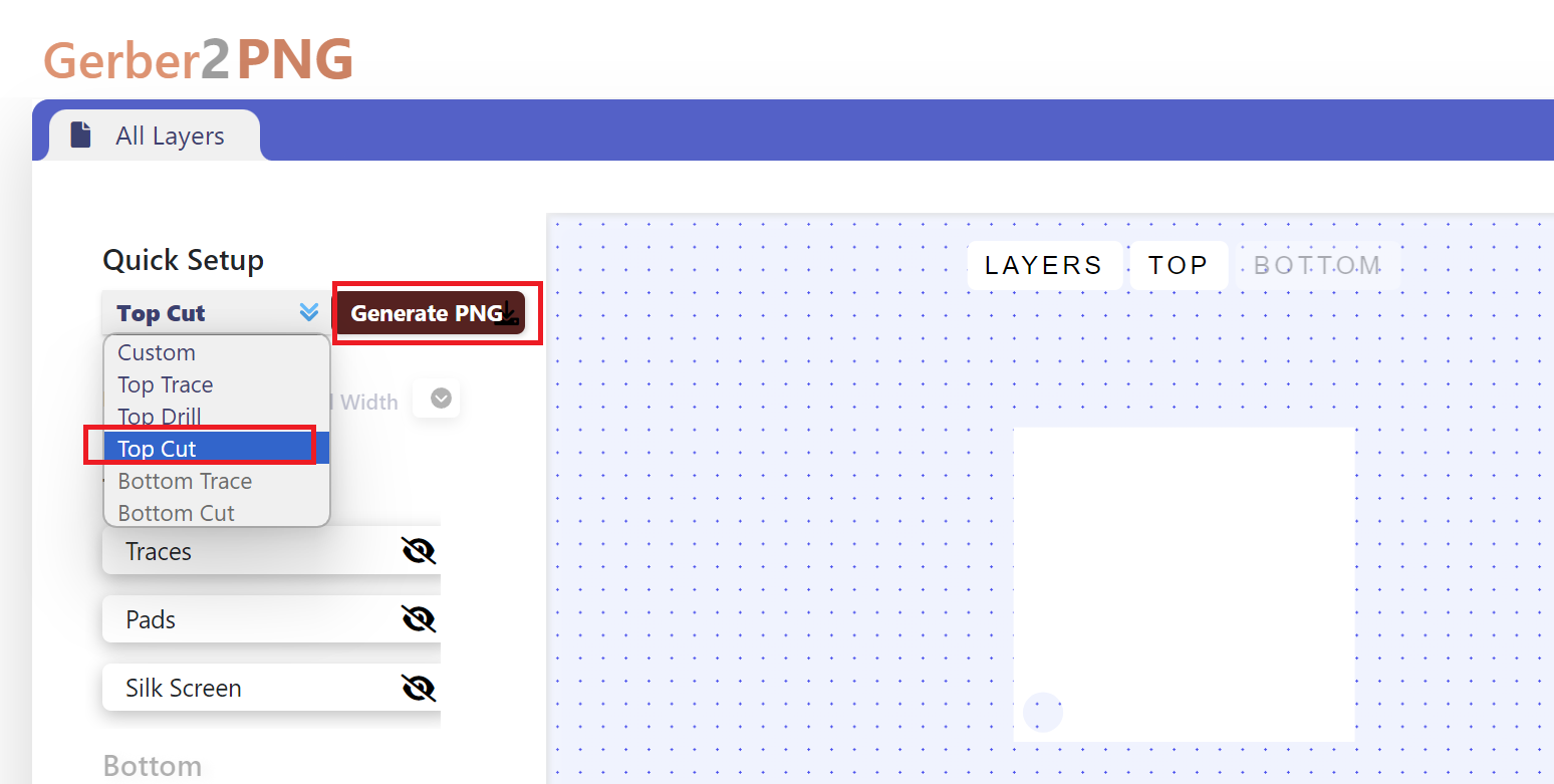
After selecting the " Generate PNG " option, the web application will generate the PNG file, visible on the right section of the browser.
You can download all the images by clicking on the download icon on the top right corner, or download them individually by clicking the download icon below each image.
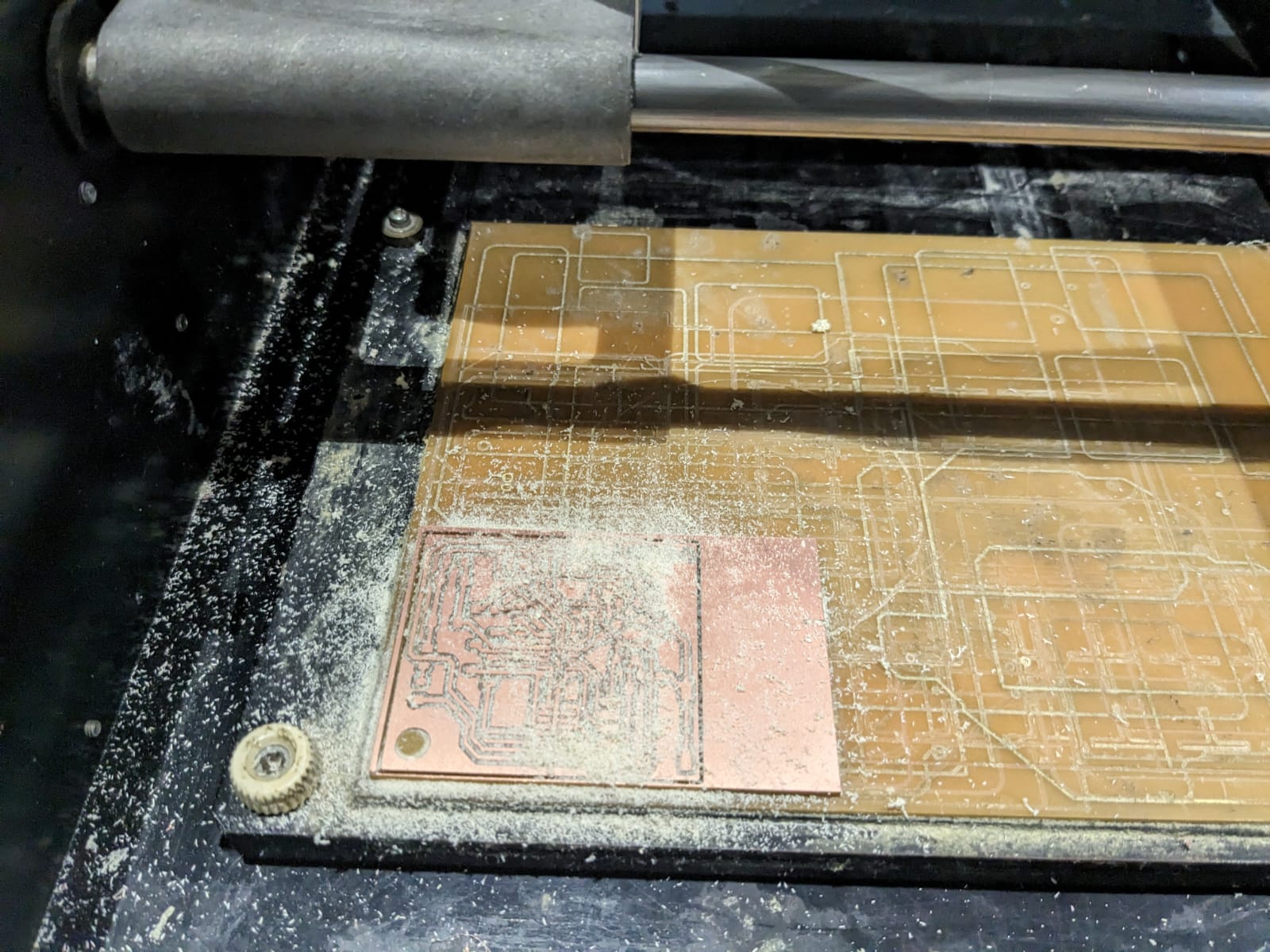
After successfully generating the PNG file for PCB milling, I proceeded to mill the PCB.
PCB Milling
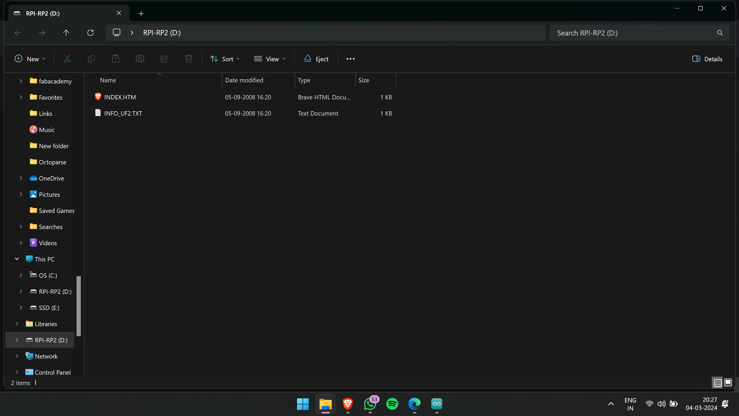
Since, both files ready for the milling process, I loaded a new PCB onto the Modalla MDX-20 milling machine
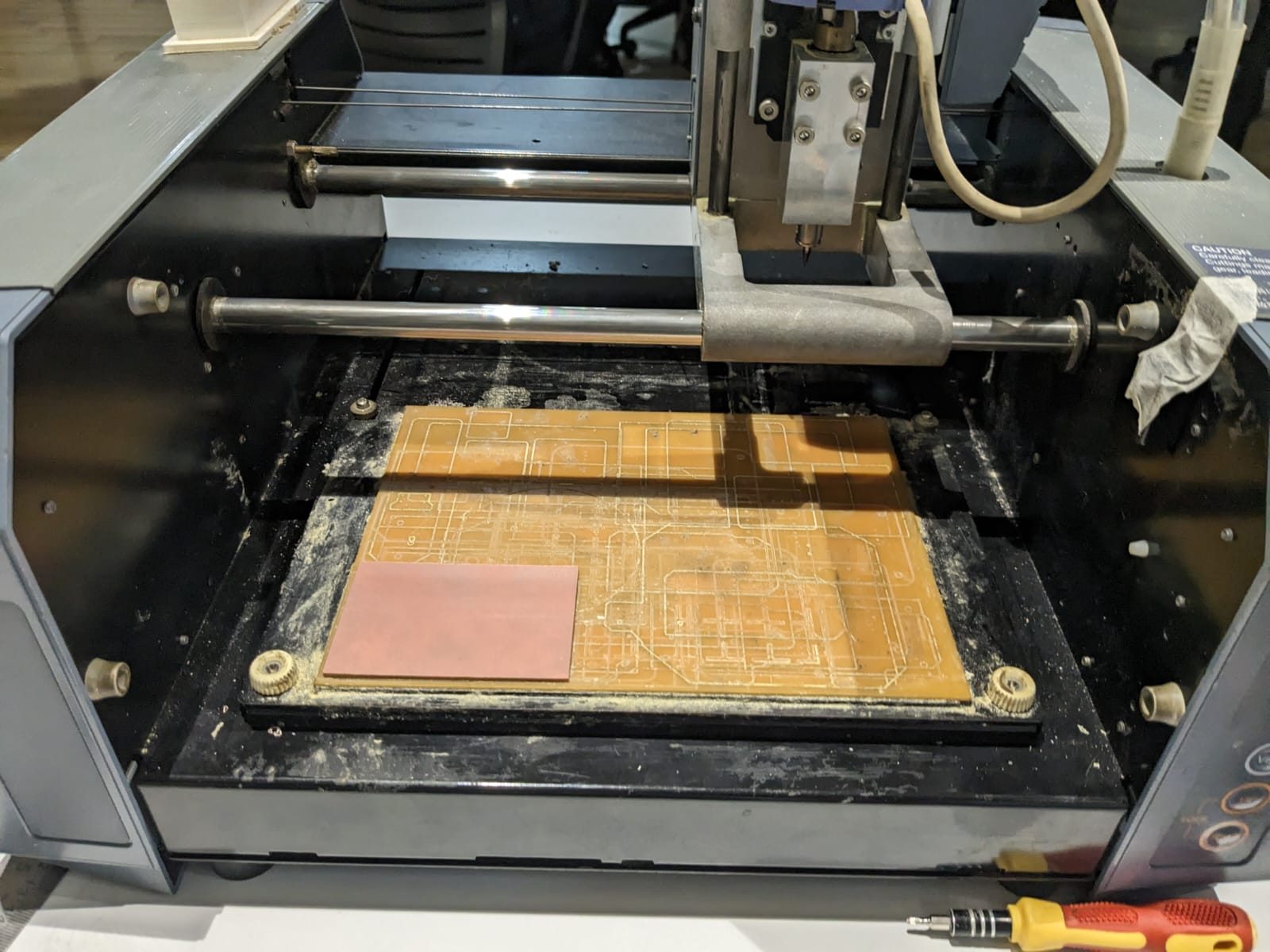
And then i opened the file in the FAB MODS software.
After loading the PCB, I followed the same steps that I had previously followed during the electronics production week.
Then i start the milling process
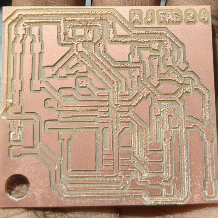
Here is the output after milling the traces
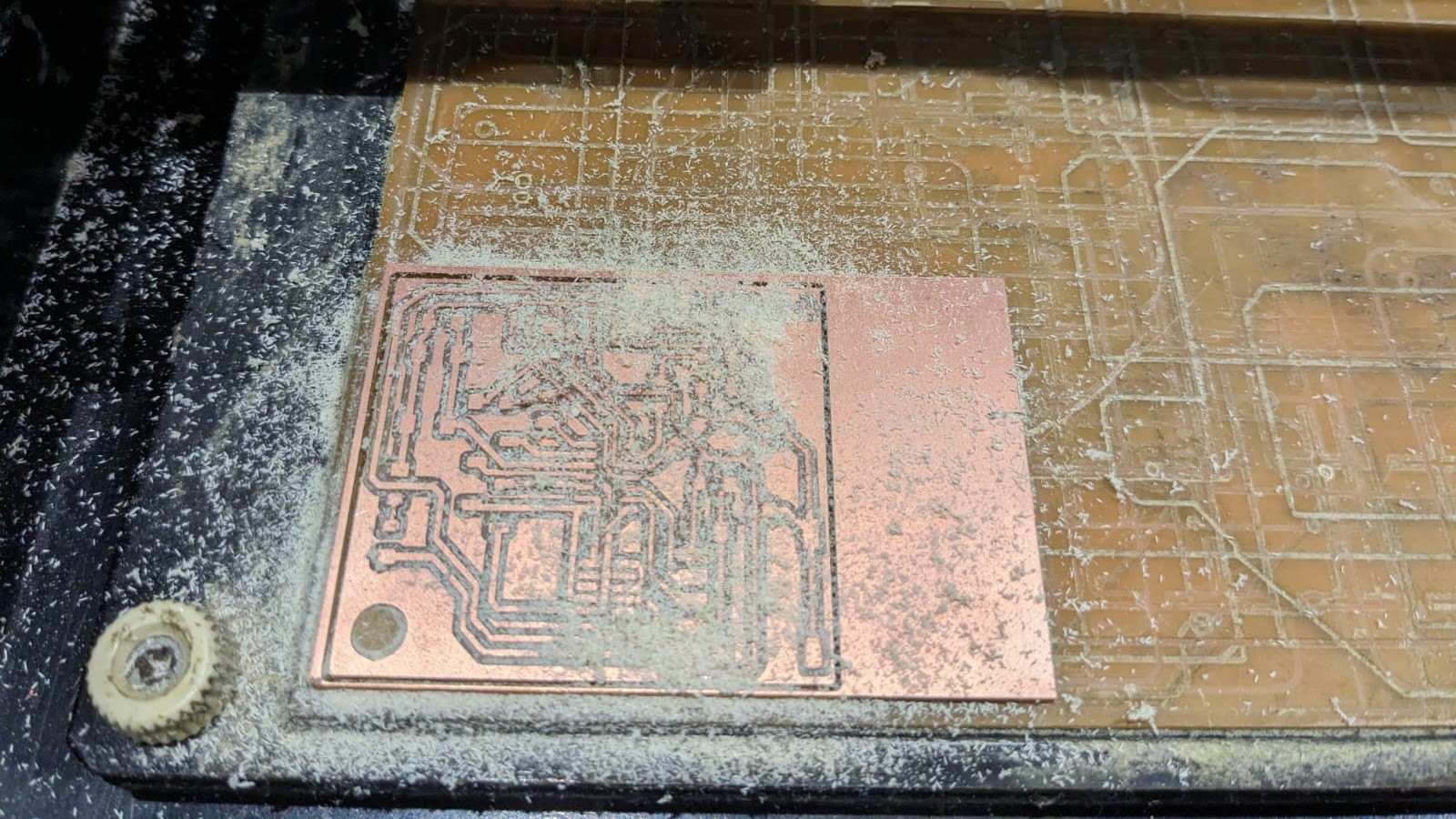
After milling the traces, I loaded the cutting file into FAB MODS and initiated the cutting process.
Here is the output after the cutting process
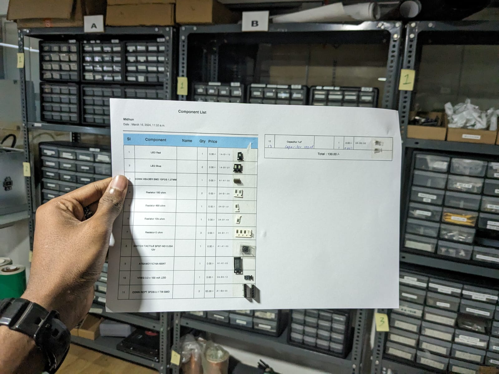
Gathering the required components.
So, now that the PCB is prepared for soldering, I have collected all the necessary components from the lab. Here's a list of the components I've gathered:
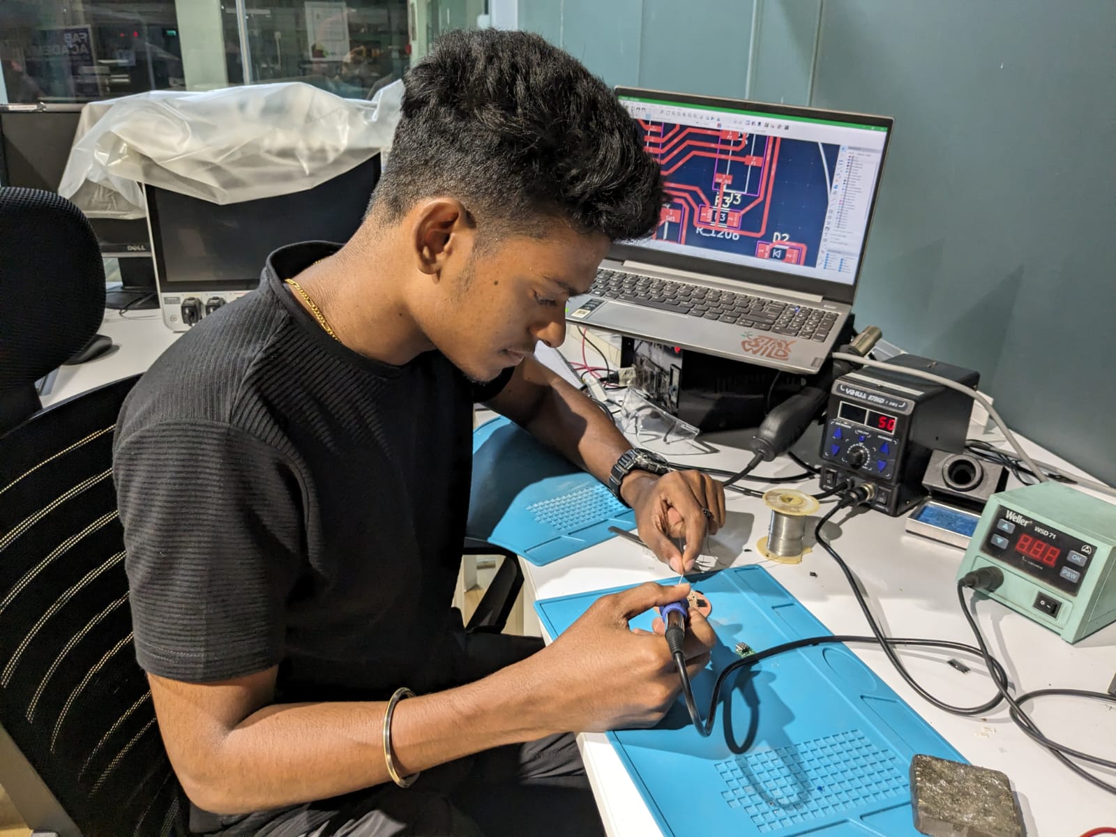
Soldering
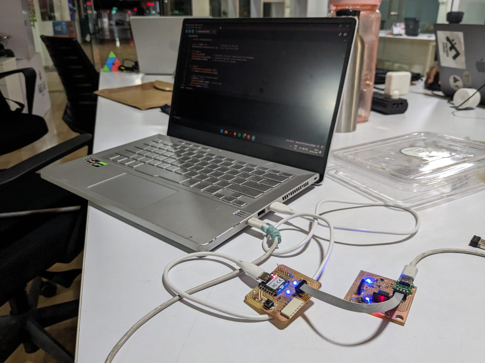
After gathering all the required components, I began soldering them into their designated places on the PCB.
Here is the result after soldering all the components into their respective places.
Hooray! I've completed the project.
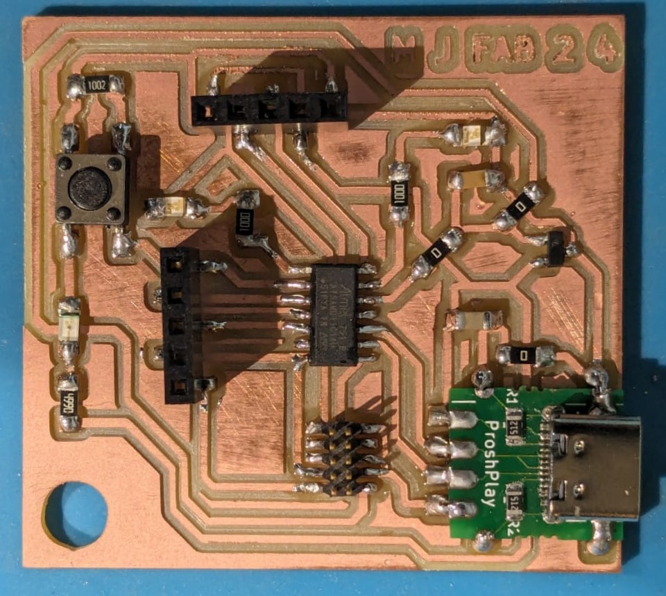
Then, I carefully inspected the PCB under a microscope for any potential shorts or soldering issues.

After checking, I didn't find any shorts on the PCB. I'm happy with the result.
Programming
Before programming the new board, it was necessary to burn the bootloade r. To accomplish this, I utilized the Quentorres board and followed the documentation for burning the bootloader.
For this task, we require the CBL RIBN 10COND 0.025 cable. Here is the cable with both ends connected to the CONN SOCKET 10POS IDC GOLD.
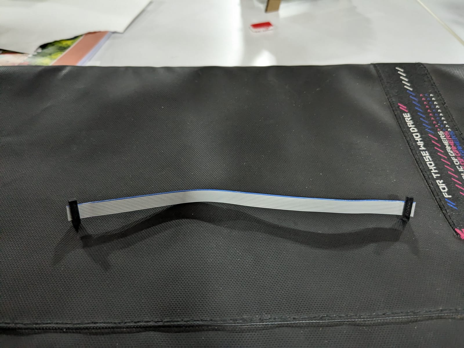
Then, I connected the SWD pin of both the Quentorres and the new board for burning the bootloader.
To burn the bootloader onto your board, begin by connecting it to your computer via a USB cable. Press and hold the "B" button, then simultaneously press and hold the "R" button. Once both buttons are pressed, release them. This action triggers the board to enter reset mode, exposing its flash memory as a hard drive.
Next, download the UF2 firmware file and transfer it to the empty hard drive that appears after completing the previous step. Once the file transfer is complete, the board will automatically reset.
Now, the Quentorres board is ready for use.
Next, I proceeded to set up the Arduino IDE platform for burning the bootloader.
Firstly, navigate to the preferences menu in the file menu of the Arduino IDE. Then, add the following link to the additional board manager URLs: https://raw.githubusercontent.com/qbolsee/ArduinoCore-fab-sam/master/json/package_Fab_SAM_index.json
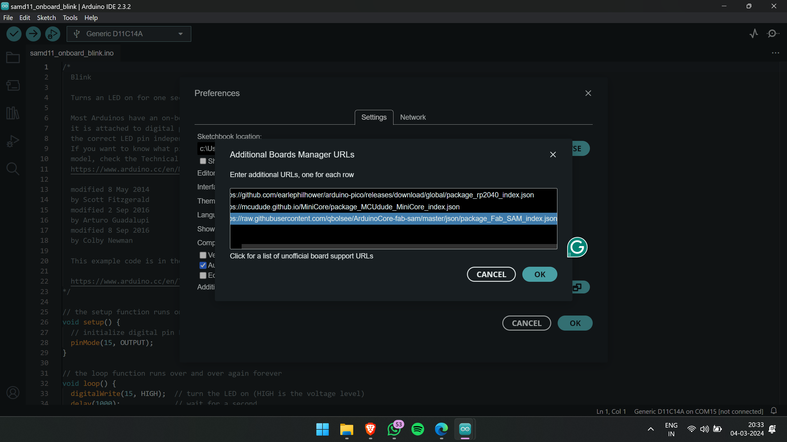
This will allow you to download the Fabcore SAM from the board manager.
After adding the link to the preferences menu and downloading the Fabcore SAM from the board manager, proceed to select the appropriate board and port in the Arduino IDE.
Once done, you can then burn the bootloader onto the board.
After successfully burning the bootloader.
Here is the pinout diagram of the board I fabricated:
The next step is to program the board.
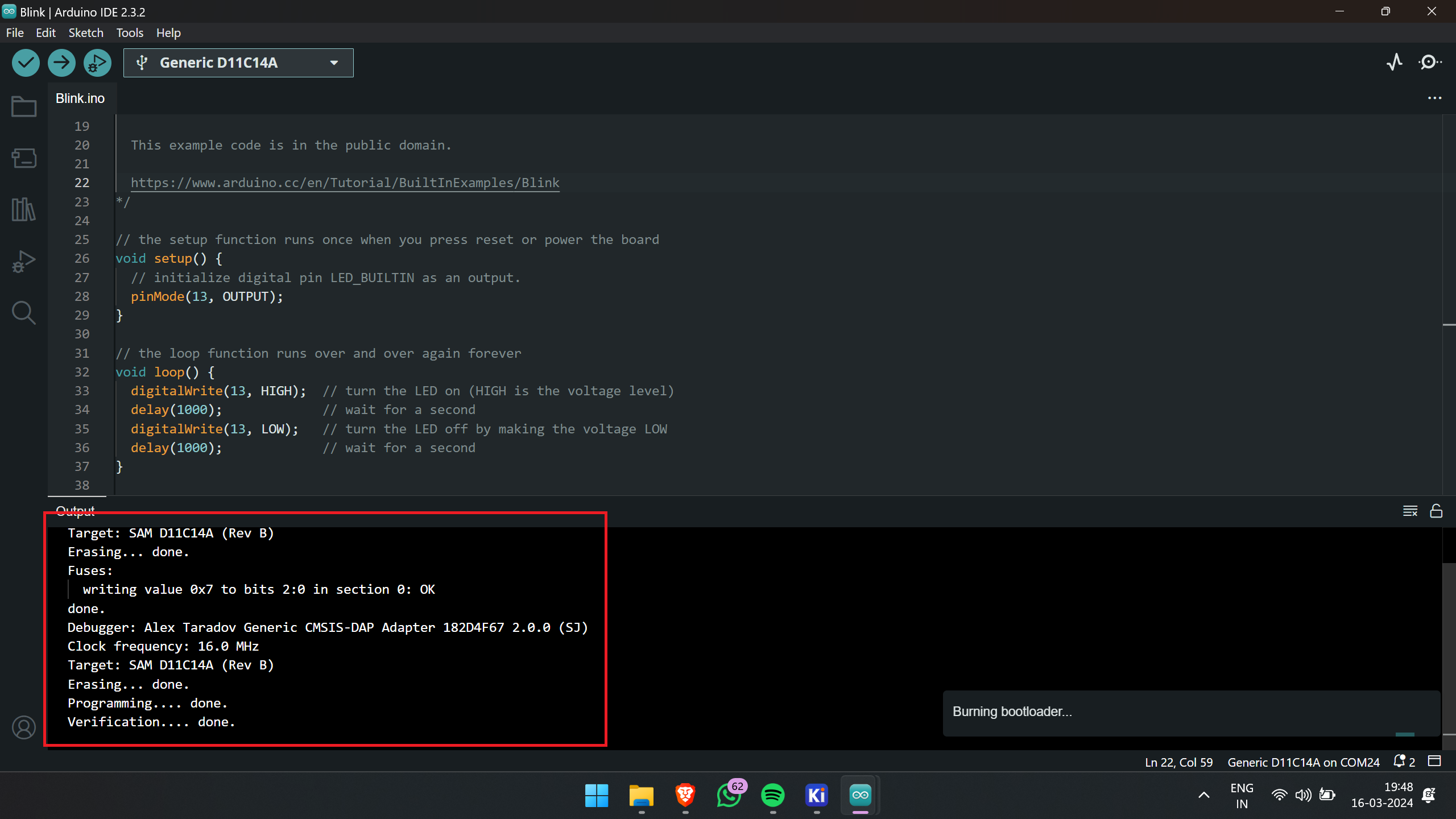
Initially, I programmed with the basic blink program from the examples menu to make the onboard LED blink.
here is the code used
void setup() {
  // initialize digital pin LED_BUILTIN as an output.
  pinMode(2, OUTPUT);
  pinMode(5, OUTPUT);
}

// the loop function runs over and over again forever
void loop() {
  digitalWrite(2, HIGH);  // turn the LED on (HIGH is the voltage level)
  delay(1000);             // wait for a second
  digitalWrite(2, LOW);   // turn the LED off by making the voltage LOW
  delay(1000);             // wait for a second
  digitalWrite(5, HIGH);  // turn the LED on (HIGH is the voltage level)
  delay(1000);             // wait for a second
  digitalWrite(5, LOW);   // turn the LED off by making the voltage LOW
  delay(1000);
}
This is how it came
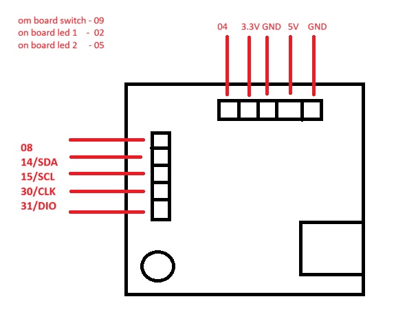
After verifying that the onboard LED was blinking correctly, I proceeded to test the push button on the board. To do this, I utilized code from examples, edited the pin number to match the one on the board, and gave it a try.
This is the code i have uploaded to the board
const int buttonPin = 09;  // the number of the pushbutton pin
const int ledPin_1 = 02;   // the number of the LED pin 1
const int ledPin_2 = 05;    // the number of the LED pin 2
int buttonState = 0;       // variable for reading the pushbutton status
bool pressed = false;
void setup() {
  pinMode(ledPin_1, OUTPUT);  // initialize the LED pin1 as an output:
  pinMode(ledPin_2, OUTPUT);  // initialize the LED pin2 as an output:
  pinMode(buttonPin, INPUT);  // initialize the button pin as an input:
}
void loop() {
  buttonState = digitalRead(buttonPin);  // read the state of the pushbutton value:
  if (buttonState == HIGH)               // check if the pushbutton is pressed. If it is, the button state is HIGH:
  {
    if (pressed == false) {
      pressed = true;
      if (digitalRead(ledPin_1) == LOW)  // check whether the led1 is off, if it is then the LEDs will be HIGH
      {
        digitalWrite(ledPin_1, HIGH);
        digitalWrite(ledPin_2, HIGH);

      }
      else {  // if led1 is on then it will turn off all the LEDs
        digitalWrite(ledPin_1, LOW);
        digitalWrite(ledPin_2, LOW);
      }
    }
  } else {
    pressed = false;
    delay(50);
  }
}
Everything works well, and here is the video output demonstrating the functionality.
Extra credits
Designing case for the PCB
Here is the case I designed in Fusion 360. I exported the STEP file from KiCad and imported it into Fusion 360. Then, I used it as a reference to design the case for the custom board.
Simulation
For simulation purposes, I utilize the Wokwi web application.
Wokwi is an online platform offering a virtual hardware simulation environment catering to electronics enthusiasts, hobbyists, educators, and students. It enables users to design, simulate, and test electronic circuits and Arduino projects directly within a web browser, eliminating the need for physical components or hardware.
This is the simulation I attempted: controlling an LED with a push button.
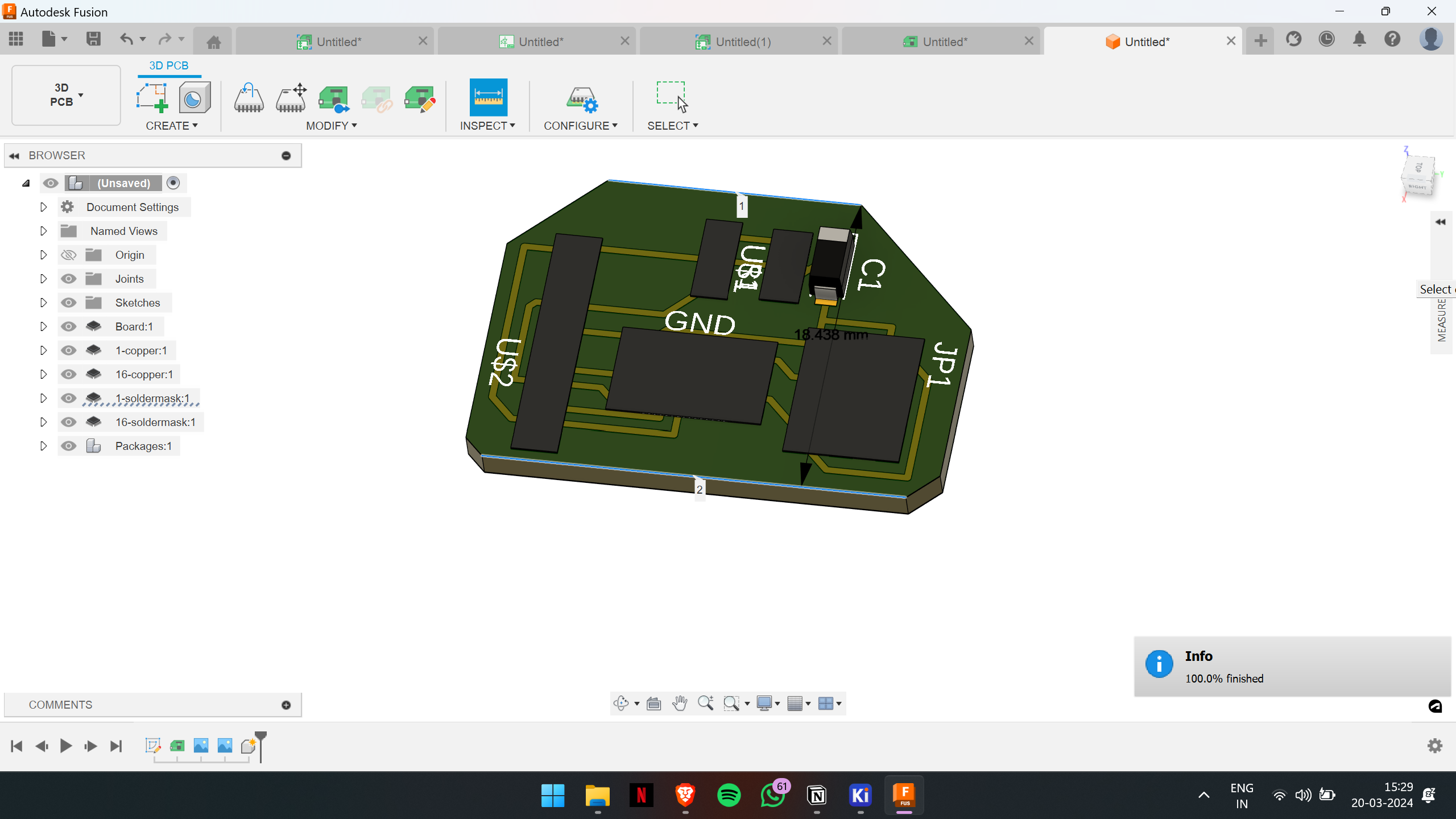
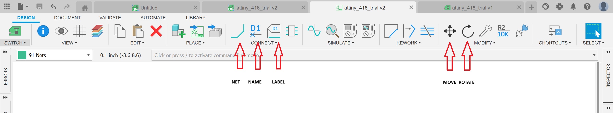
Fusion 360
I've also experimented with Fusion 360 software for PCB designing.
For designing in Fusion 360, I opted for the ATtiny412 microcontroller.
Before starting, it's important to add the Fab library. You can download the library [ https://gitlab.fabcloud.org/pub/libraries/electronics ].
To add the library, follow these steps:
- Go to the Library Pane.
- Click on "Open Library Manager."
- In the next window, navigate to "In Use" → "Browse."
- Select the file with the .libr extension.
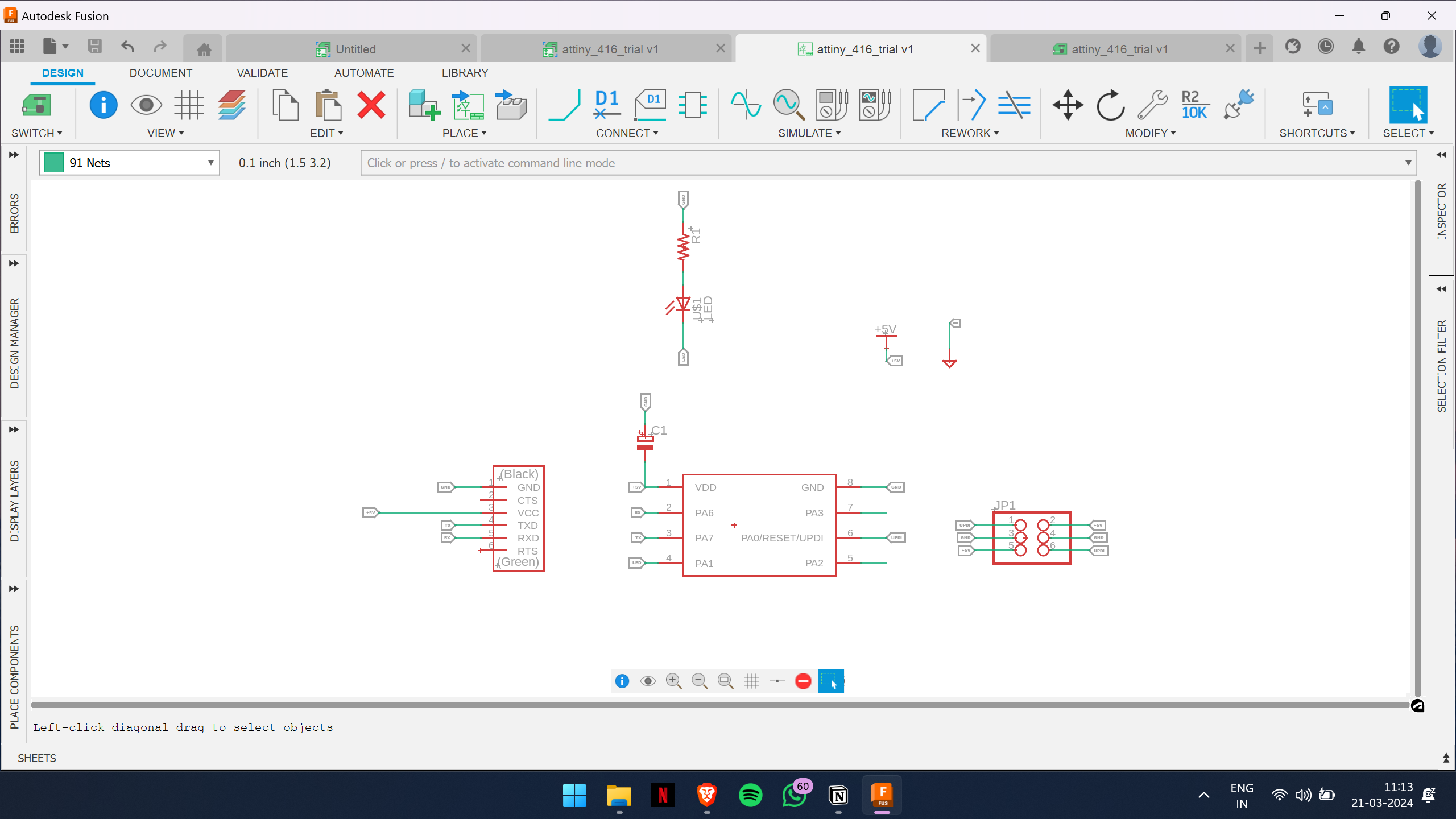
After adding the library, I started designing the schematic.
Here are the basic tools that I used to design the schematic:
Here is the simple schematic that I've designed.
After completing the schematic diagram, click on the "Switch to PCB document" icon (green icon in the top left corner).
In the new tab, adjust the canvas size and arrange the components for connecting.
We can arrange each component by using the move tool and rotate tool.
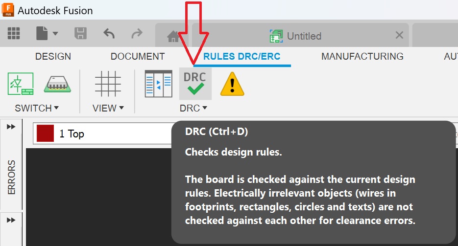
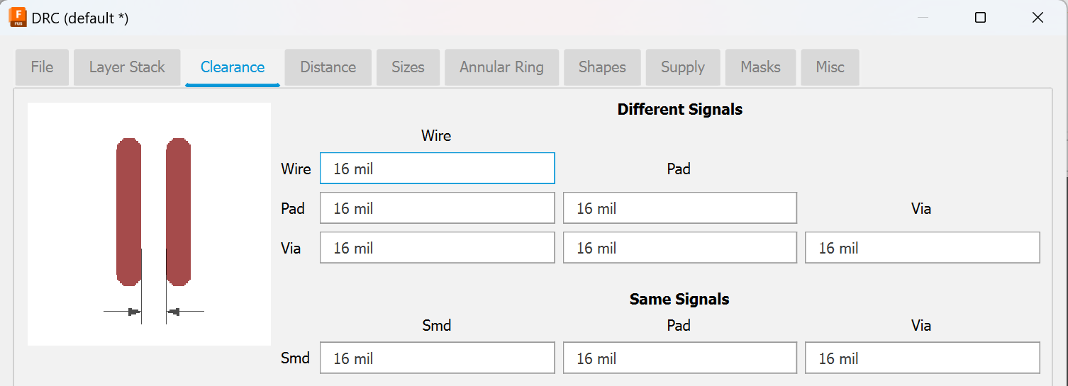
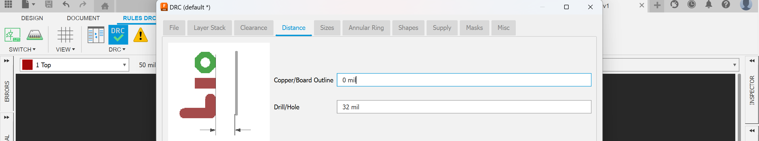
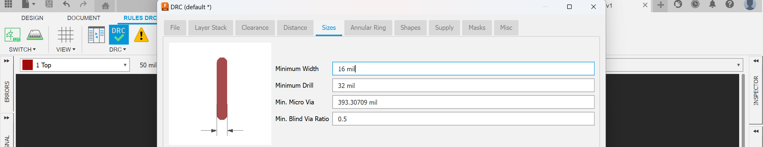
After switching to the PCB document, navigate to the RULES ERC/DRC and click on the DRC icon.
In the opening window, you can set design rules for PCB milling. Here, we use a 16 mils bit and a 32 mils bit. Set values for parameters such as clearance, hole width, etc. These will be further verified and tested during the electronics production week.
Here are the values I have configured:
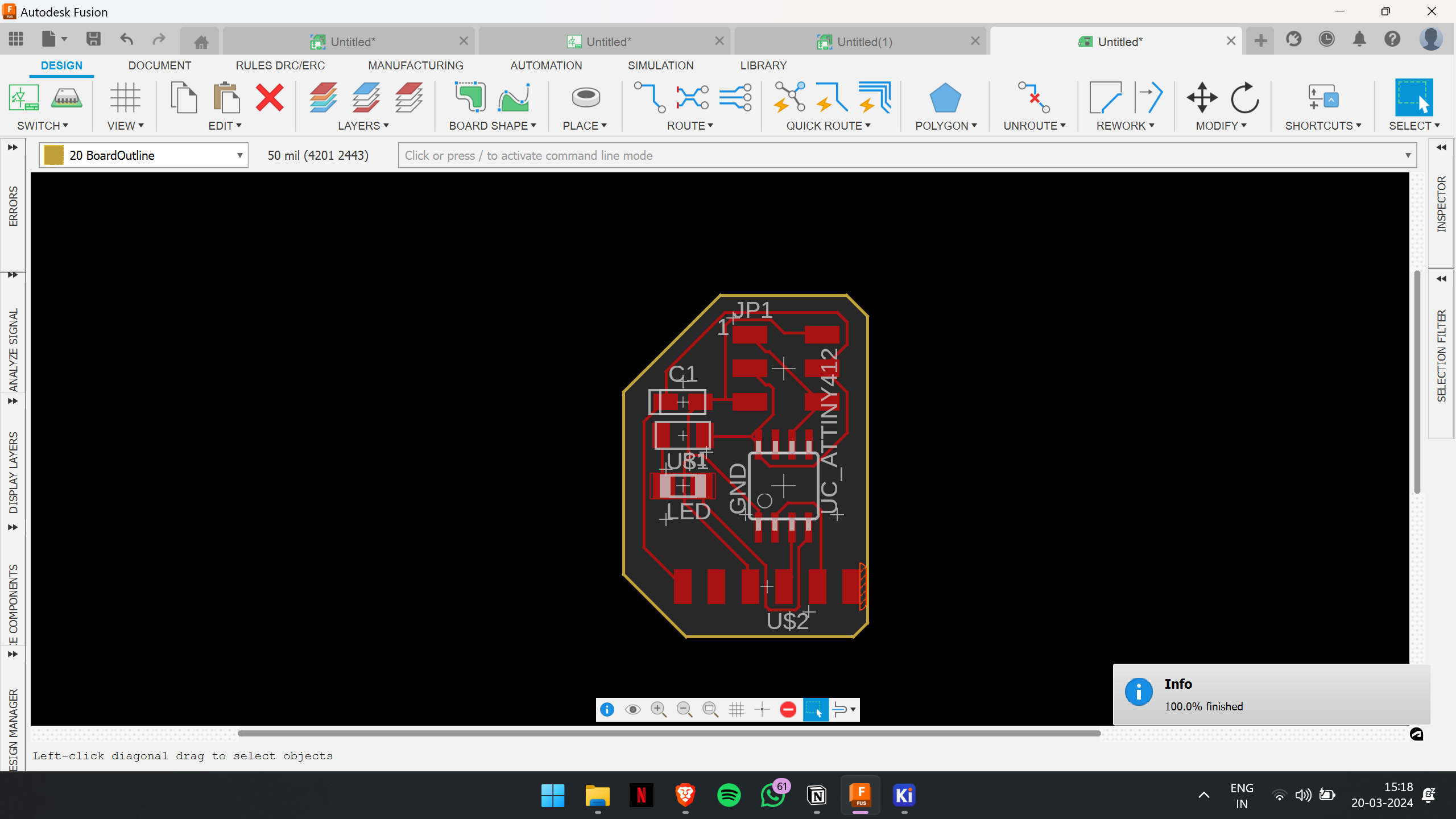
The next step is to arrange the components and route them to their correct places. Once the components are properly arranged, you can begin the routing procedure.
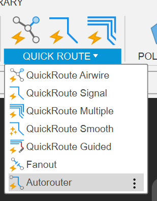
For that go to Quick Route → Auto-route.
And here is the result after auto-routing, which turned out quite well.
Additionally, you can switch to the 3D view by selecting it from the top left corner.